PAD130
Rev D
KEY FEATURES
- LOW COST ACCESSORY
- DUAL BOOST VOLTAGE OUTPUT
- WIDE SUPPLY RANGE ± 8V – ± 50V
- CONVENIENT SIP PIN-OUT
APPLICATIONS
- HIGH POWER AMPLIFIER ADD-ON
- TURNS PAD128 INTO A RAIL-TO-RAIL AMPLIFIER INCLUDING SINGLE SUPPLY OPERATION
DESCRIPTION
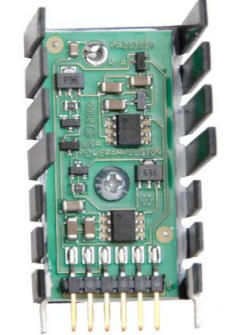
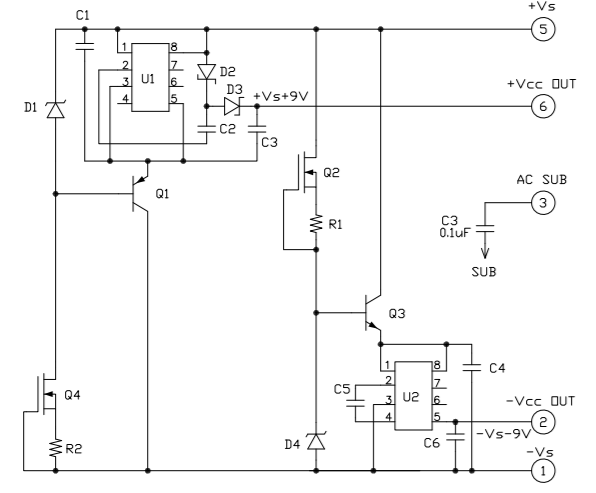
The PAD130 power supply accessory module is a compact dual switching power supply designed to provide a convenient, low-cost power supply that converts the PAD128 High Power Operational Amplifier into a RRIO amplifier (rail to rail input and rail to rail output). With input voltages of +Vs and –Vs the PAD130 produces output voltages of +Vs+9 and –Vs–9 volts. The output voltages are connected to the PAD128 +Vcc and –Vcc power supply pins. Consequently, the small signal stages of the PAD128 operate at higher voltages than the main power supply voltages, thus biasing the small signal stages such that RRIO operation is assured. The PAD130 comes mounted to a heat sink for drop-in operation.
CIRCUIT & CONNECTIONS
EQUIVALENT CIRCUIT
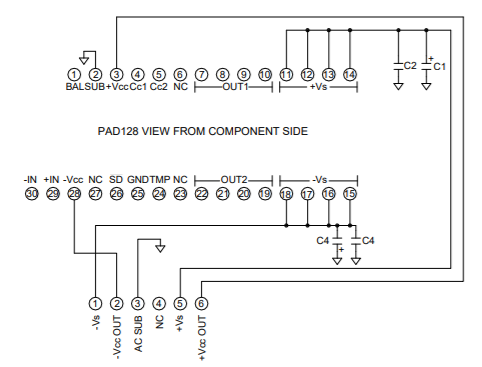
PAD130 TYPICAL CONNECTION TO PAD128
ABSOLUTE MAXIMUM RATINGS
NOTES:
- Unless otherwise noted: TC=25oC
OPERATING CONSIDERATIONS
POWER SUPPLY INPUTS
The PAD130 is normally powered by the same voltages used to power the host amplifier. The PAD130 has its own input and output filter capacitors and so no additional bypassing is necessary. A current input ripple can be observed approximately twice the output load current at a duty cycle of 50%.
The PAD130 can be operated from a single power supply voltage, for example, zero (ground) and +50V. In this case the output voltages will be approximately -9V and +58.5V.
OUTPUT VOLTAGES
The PAD130 output voltages are approximately 9V greater than the input power supply voltages. These voltages are tied to the ±Vcc inputs for the host operational amplifier (see Fig. 2) on page 2. The output voltages have some ripple at approximately 20 kHz. The host amplifier’s power supply rejection is able to reject most of the ripple amplitude but about 1 mVp-p (RTI) of residual ripple may be found at the output of the amplifier. The ripple can be reduced by adding external filter capacitors, but this is usually unnecessary.
EVALUATION KITS
Connections for the PAD130 are incorporated into the printed circuit boards included with the evaluation kits for compatible amplifiers such as the PAD128 (evaluation kit EVAL128).
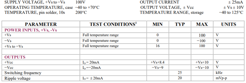
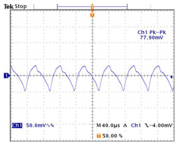
PERFORMANCE GRAPHS
+VCC OUTPUT RIPPLE
The oscilloscope display at the left shows the PAD130 +Vcc output voltage ripple. The ripple can be reduced by adding an external filtering capacitor, but the amplifier rejects a large portion of this ripple.
-VCC OUTPUT RIPPLE
The oscilloscope display at the right shows the PAD130 -Vcc output voltage ripple. The ripple can be reduced by adding an external filtering capacitor, but the amplifier rejects a large portion of this ripple. See below.
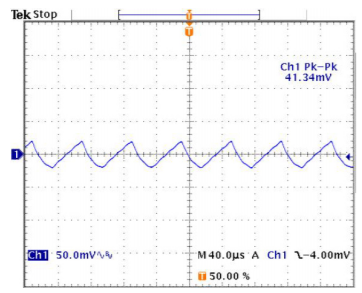
DUE TO PAD130 OUTPUT RIPPLE, G=10
AMPLIFIER OUTPUT RIPPLE WITH PAD130 POWER SUPPLY
The oscilloscope display at the left shows the PAD128 amplifier output voltage ripple due to the PAD130 power supply ripple with the amplifier in a gain of 10. The ripple is about 10mVp-p in a gain of 10. Referred to the input the ripple is about 1mVp-p. The ripple can be reduced by adding external filtering capacitors, but the amplifier rejects a large portion of this ripple as can be seen by comparing this amplifier output ripple to the power supply output ripple as seen in the oscilloscope displays above.
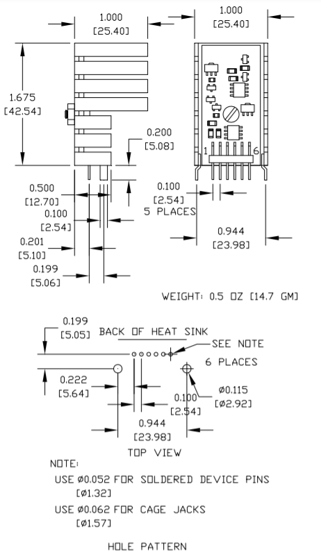
DIMENSIONAL INFORMATION