Downloads
Datasheet
PAD149 – Rev G
KEY FEATURES
- LOW COST
- HIGH VOLTAGE – 200 VOLTS
- HIGH CURRENT – 10 AMPS
- 125 WATT DISSIPATION CAPABILITY
- 100kHz POWER BANDWIDTH
- SHORT CIRCUIT PROTECTION
- TEMPERATURE MONITORING
- RoHS COMPLIANT
- CONFORMALLY COATED
APPLICATIONS
- INKJET PRINTER HEAD DRIVE
- PIEZO TRANSDUCER DRIVE
- INDUSTRIAL INSTRUMENTATION
- RELECTOMETERS
DESCRIPTION
The PAD149 is a high voltage operational amplifier constructed with surface mount components to provide a cost-effective solution for many industrial applications and especially industrial ink jet head drive. With a footprint only 3.1in2 the PAD149 offers outstanding performance that rivals more expensive hybrid component amplifiers. User selectable external compensation tailors the amplifier’s response to the application requirements. An analog output voltage is provided that is proportional to the substrate temperature. The amplifier’s output stage is shut down by pulling the shut down pin low or when the substrate temperature exceeds 110oC. A short circuit or over-current condition also shuts down the output stage. The amplifier circuitry is built on a thermally conductive but electrically insulating substrate. No BeO is used in the PAD149. The resulting module is a small, high-performance solution.
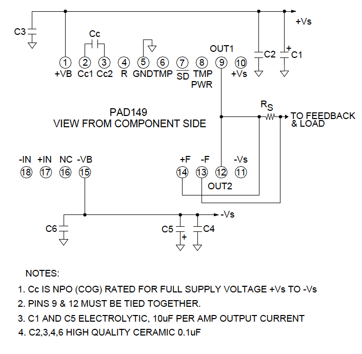
CIRCUIT & CONNECTIONS
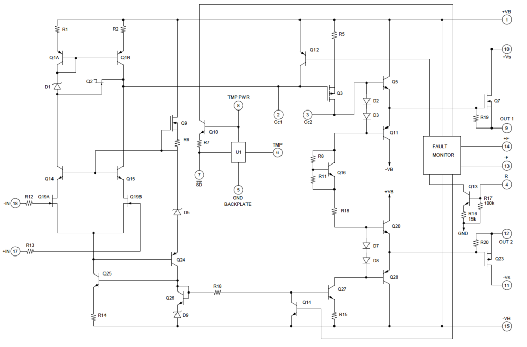
EQUIVALENT CIRCUIT
PINOUT & CONNECTIONS
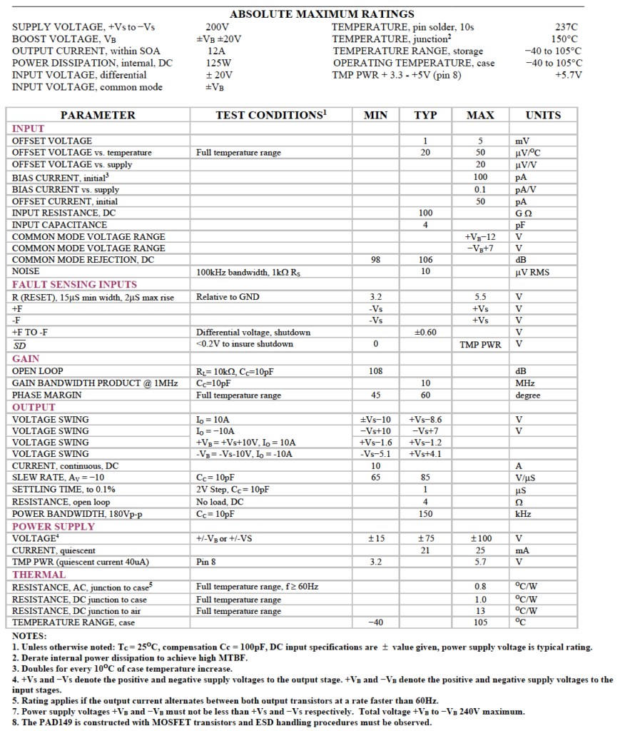
ABSOLUTE MAXIMUM RATINGS
SAFETY FIRST
The operating voltages of the PAD149 are potentially deadly. When developing an application circuit, it is wise to begin with power supply voltages as low as possible while checking for circuit functionality. Increase supply voltages slowly as confidence in the application circuit increases. Always use a “hands off” method whereby test equipment probes are attached only when power is off.
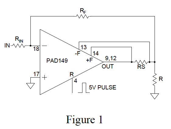
OVER-CURRENT FAULT PROTECTION
The output stage of the PAD149 is shut down when an over- current fault is detected. The protection circuit monitors the voltage across an external sense resistor, Rs. The fault condition set point is programmed by:
IF = 0.6V/RS
Where IF is the value of the fault current set point and RS is the value of the sense resistor.
Whenever the programmed current set point is exceeded for more than 10 μS (typical) the drive to the output stage turns off completely (typically in less than 10μS), and remains off until the circuit is reset (pin 4, R) via a 5V momentary pulse ≥ 15μS (or power recycled). The internal sense voltage is approximately 0.6V and decreases about 2.2mV/ oC of substrate temperature rise. For some loads a start-up current may exceed the normal programmed maximum value. This condition should be considered when setting the programmed fault value. See Figure 1, below, for a typical over-current fault connection diagram.
MOUNTING THE AMPLIFIER
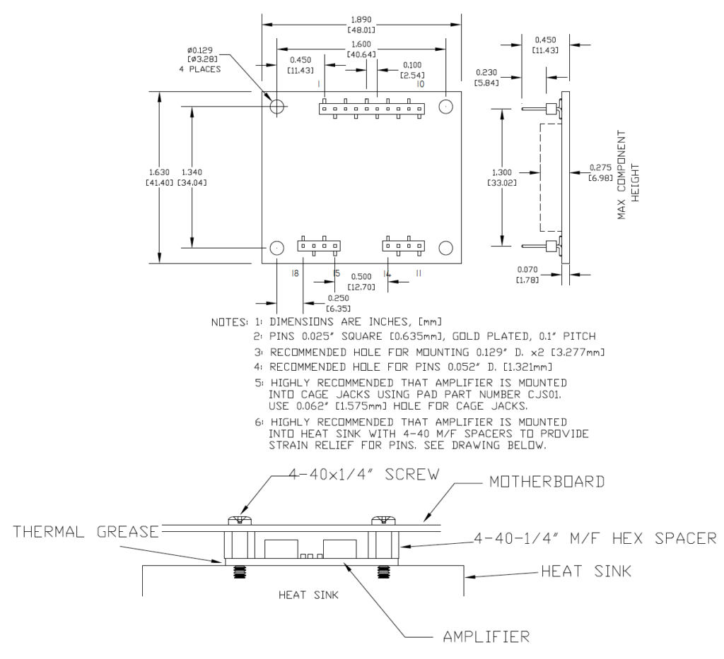
In most applications the amplifier must be attached to a heat sink. Spread a thin and even coat of heat sink grease across the back of the PAD149 and also the heat sink where the amplifier is to be mounted. Push the amplifier into the heat sink grease on the heat sink while slightly twisting the amplifier back and forth a few times to bed the amplifier into the heat sink grease. On the final twist align the mounting holes of the amplifier with the mounting holes in the heat sink and finish the mounting using 4-40 hex male-female spacers. Mount the amplifier to the mother board with 4-40 X 1/4” screws.
PHASE COMPENSATION
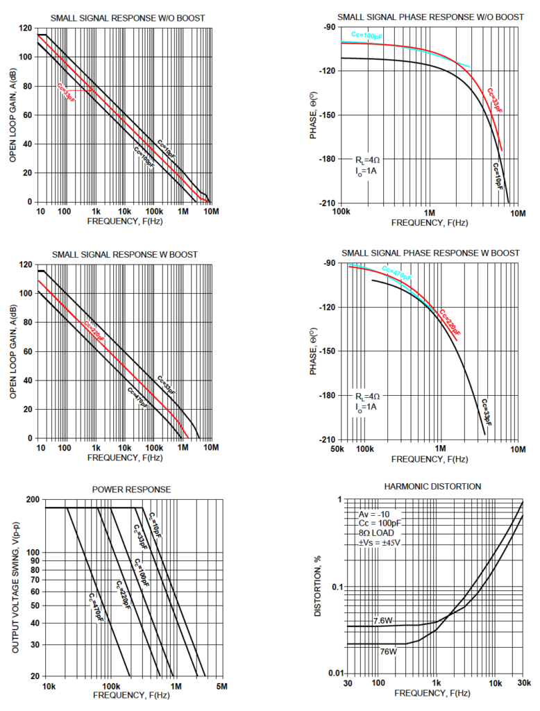
The PAD149 must be phase compensated. The compensation capacitor, CC, is connected between pins 2 and 3. The compensation capacitor must be an NPO type capacitor rated for the full supply voltage (200V). On page 2, under Amplifier Pinout and Connections, you will find a table that gives recommended compensation capacitance value for various circuit gains and the resulting slew rate for each capacitor value. Consult also the small signal response and phase response plots for the selected compensation value in the Typical Performance Graphs section. Do not use a compensation capacitor less than 10pF.
MOUNTING THE AMPLIFIER
The amplifier is supplied with four 4-40 M/F hex spacers at the four corners of the amplifier. Since the male threaded ends of the spacers extend beyond the amplifier pins the spacers provide a convenient alignment tool to guide the insertion of the amplifier pins into the circuit board. Once the amplifier is seated secure the module with the provided 4-40 nuts and torque to 4.7 in lb [53 N cm] max. See “Dimensional Information” for a detailed drawing. It is recommended that the heat sink be grounded to the system ground. This can easily be done by providing a grounded circuit board pad around any of the holes for the mounting studs.
TEMPERATURE REPORTING
An analog output voltage is provided (pin 6, TMP) relative to ground (PIN 5) and proportional to the temperature in degrees C. The slope is approximately -10.82mV/oC. The output voltage follows the equation:
T = (2.127 ─ V) (92.42) or
V = 2.127 ─ (T/92.42)
Where V is the TMP output voltage and T is the substrate temperature in degrees C.
THERMAL SHUTDOWN
The temperature monitoring circuit automatically turns off the output transistors when the substrate temperature reaches 110oC. The output remains disabled until the substrate temperature falls below 100oC and the circuit is reset (R, pin 4). The thermal shutdown feature is activated by amplifier thermal overload such as sustained high power dissipation or inadequate heat sinking.
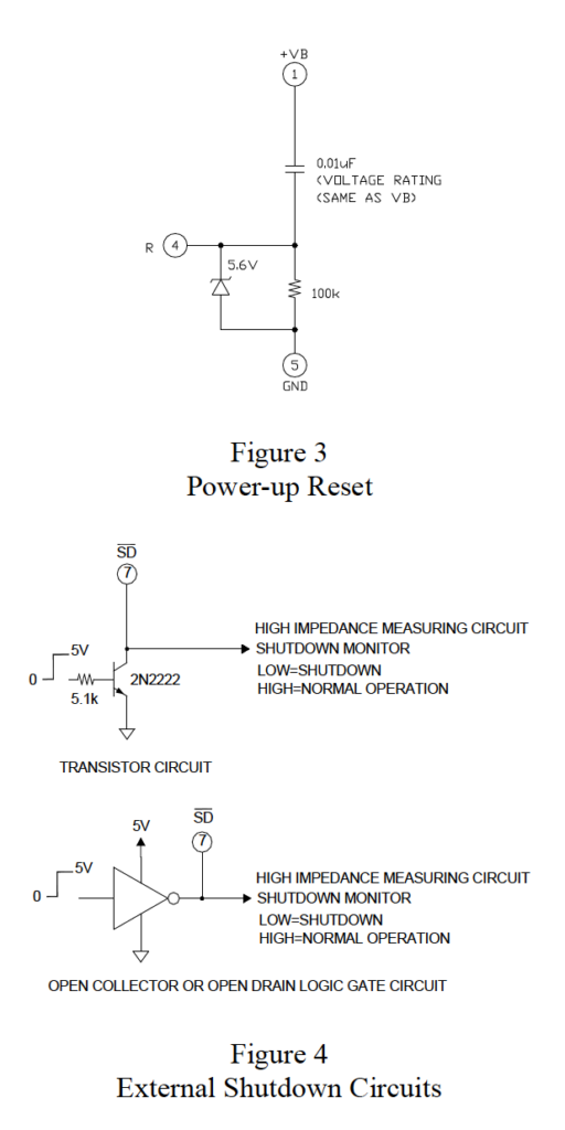
EXTERNAL SHUTDOWN
When pin 7 ( ) is taken low (GND) the output stage is turned off and remains off until reset pulse at pin 4 (R) is applied, or power to the amplifier is restarted. If the pin is monitored with a high impedance circuit (>100k input impedance) it also gives an indication of the temperature status of the amplifier. A “high” indicates normal temperature operation and a “low” (zero volts, approximately) indicates that the amplifier is shut down due to the occurrence of an over-temp condition. A “high” will be the approximately the same voltage as TEMP PWR (pin 8). See Figure 4 in Applications, page 10, for external shutdown circuits.
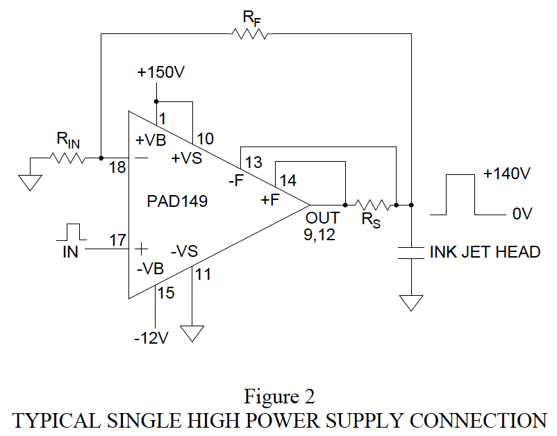
SINGLE HIGH POWER SUPPLY OPERATION
The small signal stages of the PAD149 are connected in such a way that the output stage can be powered by a single high- power supply voltage. -VB needs to be connected to a negative voltage so that the amplifier’s input common mode voltage conditions are satisfied. But the output stage can be connected between ground at -Vs and a high voltage supply at +Vs. The amplifier is then biased so that the amplifier’s output stage can swing close to ground. This technique is often used to operate the amplifier with only a single high current power supply, thus reducing the system size and cost. See Figure 2 below.
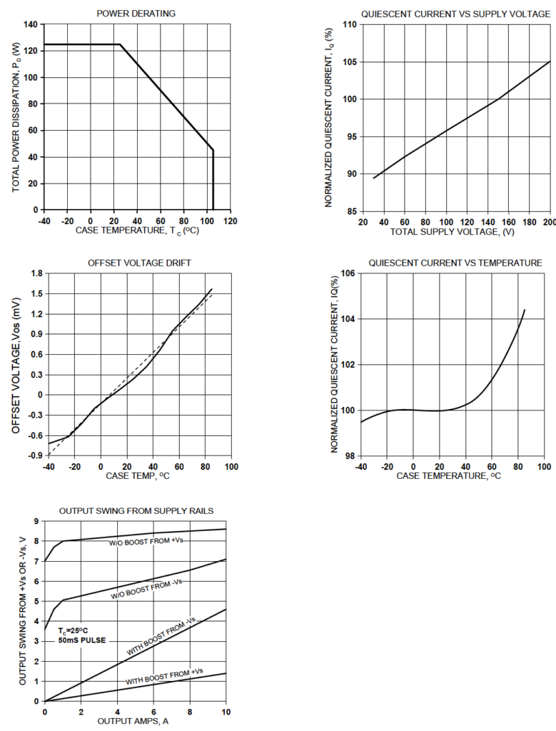
PERFORMANCE GRAPHS